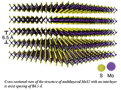
 Multilayered transition metal dichalcogenides (TMDs), such as MoS2, fall within a class of 2D materials that may exhibit remarkable optical, electronic, and structural properties depending on the interactions both within and between atomic layers. A number of “impurity” methods—doping, intercalation, and site defects, for example—have been exploited in an effort to modify the material properties of MoS2. At HPCAT, group of researchers from the University of Texas at Austin, the Chinese Academy of Sciences, and the Indian Institute of Science recently took an alternative approach by applying high pressure to high-purity samples of multilayered MoS2.
Based on several complementary experimental techniques, the results demonstrate a pressure-induced semiconducting-to-metallic transition at approximately 19 GPa. Furthermore, synchrotron powder x-ray diffraction measurements, carried out in part at HPCAT, reveal only a slight lattice distortion across the phase transition. These experimental results, together with extensive theoretical calculations, strongly suggest that this transition is between two electronic states, characterized by pressure-induced charge localization around the Mo atoms, which in turn gives rise to increased interaction between neighboring layers of sulphur atoms [Nayak et al., Nature Comm., 5, 3731 (2014)].
